PARADIM provides a world-class user facility for the discovery of new electronic materials. This is built upon a strong foundation of existing materials growth and characterization equipment, supplemented by significant new facilities made possible by the NSF-Materials Innovation Platform (MIP) funding (PARADIM, DMR-2039380). PARADIM has the most advanced and complete set of openly available equipment and expertise in the world for the discovery of new inorganic materials in thin film or bulk form.
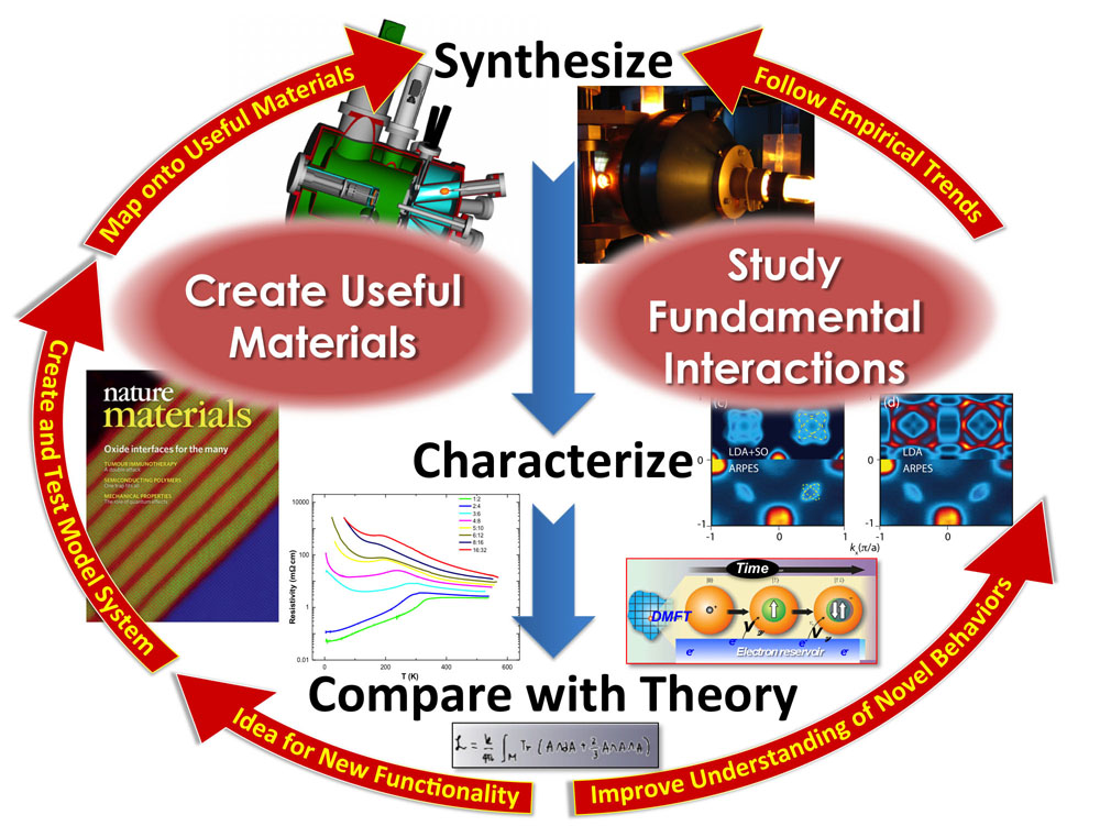
PARADIM is an NSF Materials Innovation Platform providing facilities for materials-by-design for both bulk and thin film materials. PARADIM supports the materials by design philosophy through 4 state of the art user facilities.
Bulk Crystal
The PARADIM Bulk Crystal Growth Facility is located at Johns Hopkins University. Together with the thin film growth facilities at Cornell, it provides unprecedented capabilities for discovery of new materials and interfaces.
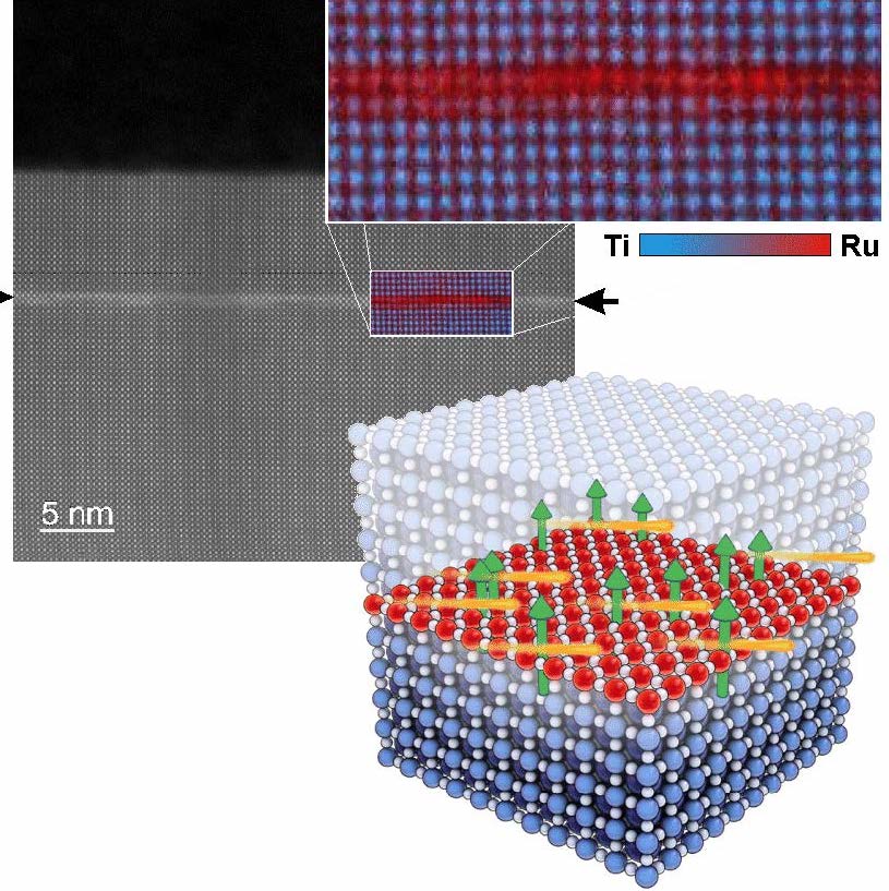
Electron Microscopy
Critical to evaluating new materials is the ability to resolve extremely fine physical features, especially the structure of interfaces, defects and strained thin films.
Theory & Simulation
Theory and Simulation are a critical part of the Materials by Design process employed by PARADIM.
Thin Film Growth
The PARADIM Thin Film Growth Facility provides unprecedented capability for the growth and characterization of thin films and interfaces of inorganic materials.
Additional characterization and fabrication resources via CCMR, CHESS, and CNF at Cornell
New Capabilities announced at the 2020 PARADIM User meeting webinar, December 16, 2020 !
PARADIM facilities are open to all US scientists via a reviewed proposal process.