PARADIM’s electron microscopy (EM) facility leverages and expands on existing capabilities in the Cornell Center for Materials Research (CCMR, a research center that includes an NSF-funded Materials Research Science and Engineering Center, MRSEC DMR-1719875) giving users access to a unique set of advanced analysis tools for materials characterization.
Critical to evaluating new materials is the ability to resolve extremely fine physical features, especially the structure of interfaces, defects and strained thin films. While conventional transmission electron microscopes (TEMs) are available for sample screening, advanced techniques such as atomic resolution imaging and spectroscopy can be performed on two aberration-corrected S/TEMs. The Nion ultraSTEM 100 was the first of a new generation of electron microscopes designed for room temperature chemical analysis and imaging at the atomic scale. With almost a nano-Amp of current focused into a subatomic electron beam, it can form atomic-resolution images of composition and bonding in under a minute. The microscope was designed to correct all geometric aberrations out to fifth order, reducing chromatic aberrations and energy spread. Combined with a cold field emission gun and an efficiently coupled spectrometer, this instrument is optimized for high spatial resolution electron energy loss spectroscopy (EELS). Atomic resolution analysis on the UltraSTEM is, however, limited to room temperature operation. A more recently installed cryo-STEM, a customized FEI Titan Themis 300 funded through the NSF-MRI program (MRI-1429155), offers a unique opportunity to expand the phase space accessible for quantitative analysis. It provides low-temperature capabilities not available anywhere else. This monochromated instrument operates as both a TEM and aberration corrected STEM from 60-300 keV, with a high-speed GIF Quantum for EELS mapping. It is equipped with a Lorentz lens for magnetic imaging, and is compatible with a range of available in-situ TEM holders for sample heating, cooling and electrical biasing.
An additional side-entry TEM, Tecnai F20 TEM/STEM, serves as training tool, for sample screening, and for grain size characterization in 2D materials. The cryo-enabled Tecnai F20 TEM/STEM is equipped with a monochromator and a spectrometer, and is used for electron tomography and ultra-high energy resolution spectroscopy – allowing optical spectroscopy at nm spatial resolution and 100 meV energy resolution.
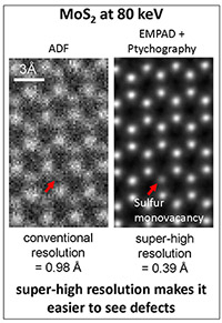
A novel electron microscopy pixel array detector (EMPAD), developed at Cornell, is available on the FEI Titan Themis. It displays single electron sensitivity, and an unparalleled 106 dynamic range. On the aberration corrected STEM, the EMPAD allows users to map electric and magnetic fields simultaneously with pm-precision measurements of the underlying atomic structure.
Rapid sample characterization including assessment of crystal orientation and strain relaxation, is performed on a Mira SEM with EBSD/orientational imaging system, and a b-Nano airSEM for high throughput SEM and EDX. TEM samples are prepared using a FEI Strata 400 dualbeam FIB, with fastloader and modified for low-energy operation, or the Helios G4 UX Focused Ion Beam (FIB). The latter is equipped with Thermo-Fisher’s most advanced ion column enabling high-resolution imaging even at low milling voltage that are critical for the production of high-quality lamella with minimal damage layers for TEM. Additionally, the beam currents now extend three times higher than previously available, enabling milling of samples not previously possible due to realistic time constraints.
Lorentz microscopy can be performed on the both F20and the Titan Themis. It provides PARADIM’s electron microscopy users access to imaging the magnetic domain structure of their samples.
Preview of New Capabilities
PARADIM’s staff scientist for electron microscopy, Don Werder (djw326@cornell.edu), assists and guides users in the operation of the instruments, with a goal of training them towards independent operation and skills they can transfer to their home institutions. Don has been trained in advanced imaging techniques including Lorentz microscopy, EMPAD imaging and cryogenic imaging.
These electron microscopy facilities are part of the Cornell Center for Materials Research but can be accessed via the PARADIM user program. Reviewed and approved PARADIM user projects receive access to the facilities and to imaging and sample preparation support from PARADIM staff. As with other PARADIM resources, access is without charge to approved US academic and government projects. Preference will be given to projects in which characterization is part of larger materials by design effort.
The electron microscopy facility is directed by Prof. Lena Kourkoutis with user support from Don Werder, PARADIM staff scientist. Please contact them with specific questions on capabilities.