PARADIM Highlight #83—Local User Project (2023)
Judy J. Cha and Lena F. Kourkoutis (Cornell), Yimei Zhu (BNL), Peijun Gou (Yale), Yanbing Zhu, Felipe Jornada, and Evan J. Reed (Stanford)
In layered van der Waals (vdW) solids, exotic quantum phenomena can be engineered via the layer stacking. For instance, the twist angle in bilayer graphene influences the low-energy electronic band structure, allowing for control over magnetic, superconducting, and topological phases. An additional control parameter is the in-plane displacement between layers, i.e., the layer stacking order. Here, PARADIM’s electron microscopy facility is used to directly visualize the in-plane displacement—the inter-layer shift (red and green arrows) of MoTe2.
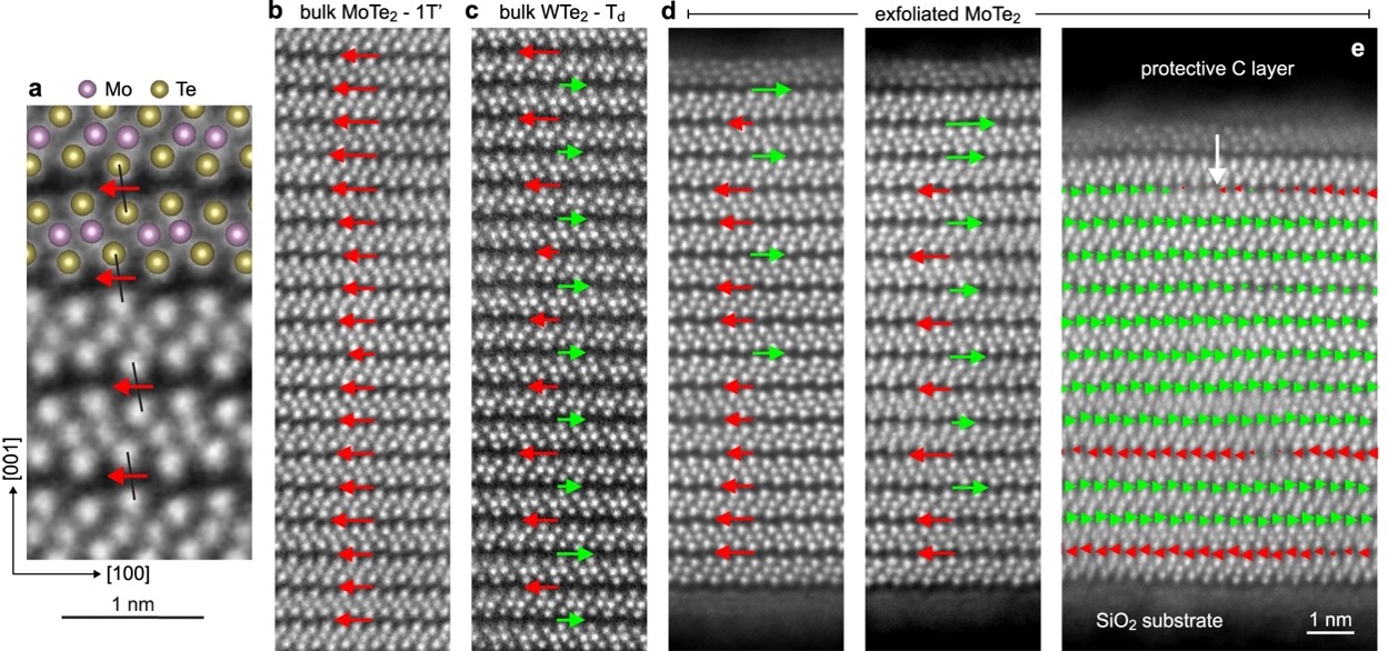
Figure 1: Cross-section atomic-resolution imaging of MoTe2 and WTe2. a) Magnified HAADF-STEM image of bulk MoTe2 with overlaid atomic structure. The black lines show the bridging Te-Te pairs and the red arrows represent the inter-layer shift b-e) HAADF-STEM images of bulk MoTe2 and WTe2, and exfoliated thin film MoTe2 respectively, with overlaid arrows representing the average value of the inter-layer shift.
For the 1T’ phase of MoTe2 all displacement points in the same direction (b). In stark contrast, a 9-nm-thin flake of MoTe2 scrambling of the displacement (d to e); the stacking lacks long-range order and appears highly disordered and even changes in stacking direction are observed (white arrow in e).
The study raises important questions regarding the electronic structure, topology, and charge transport mechanisms in exfoliated TMD flakes, and how thickness may influence layer stacking in other 2D materials which exhibit stacking-dependent functionality, e.g., magnetic 2D materials. This work also highlights the importance of atomic-scale analysis in determining the structure of 2D materials.
The layer stacking in 2D materials strongly affects functional properties and holds promise for next-generation electronic devices. In bulk, octahedral TMDs possess two stacking arrangements, the ferroelectric Weyl semimetal Td phase and the higher-order topological insulator 1T′ phase. However, in thin flakes of MoTe2, it is unclear if the layer stacking follows the Td, 1T′, or an alternative stacking sequence. Here, we use atomic-resolution scanning transmission electron microscopy to directly visualize the MoTe2 layer stacking. In thin flakes, we observe highly disordered stacking, with nanoscale 1T′ and Td domains, as well as alternative stacking arrangements not found in the bulk. We attribute these findings to intrinsic confinement effects on the MoTe2 stacking-dependent free energy. Our results are important for the understanding of exotic physics displayed in MoTe2 flakes. More broadly, this work suggests c-axis confinement as a method to influence layer stacking in other 2D materials.
The study of 2D transition metal dichalcogenides (TMDs) has largely assumed that the layer stacking in the nanoscale limit adopts one or more of the possible precise stacking sequences found in bulk specimens. This work demonstrates – via atomic resolution imaging – that in fact much greater stacking complexity arises in the thin limit than previously assumed. Given the importance of interlayer stacking on electronic, magnetic, and optical properties, this result suggests greater study of stacking is needed during the characterization of 2D TMDs.
PARADIM’s user facility for electron microscopy at Cornell University provided access to high-resolution STEM capabilities including advanced sample preparation, to visualize the inter-layer stacking.
The work was initialized by a group from Yale University (Judy Cha, before moving to Cornell) and includes collaborators for materials growth at Brookhaven National Lab as well as for ab initio calculations at Stanford University and Raman spectroscopy at Yale University.
J.L. Hart, L. Bhatt, Y. Zhu, M.-G. Han, E. Bianco, S. Li, D.J. Hynek, J.A. Schneeloch, Y. Tao, D. Louca, P. Guo, Y. Zhu, F. Jornada, E.J. Reed, L.F. Kourkoutis, and J.J. Cha, "Emergent layer stacking arrangements in c-axis confined MoTe2," Nat. Commun. 14, 4803 (2023).
Data Access:
The PARADIM Data Collective (PDC) provides access to the electron microscopy data collected at the platform via the Data DOI: 10.34863/bm64-9w84.
J.L.H. and J.J.C. were funded through the Gordon and Betty Moore Foundation’s EPiQS Initiative, grant GBMF9062.01. The work at the University of Virginia has been supported by the Department of Energy, Grant number DE-FG02-01ER4592. S.L. and P.G. acknowledge the support from the Air Force Office of Scientific Research (Grant No. FA9550-22-1-0209). The work at BNL is supported by the Office of Basic Energy Sciences, Materials Sciences and Engineering Division, U.S. DOE under Contract No. DE-SC0012704. Device fabrication was performed in part at the Cornell NanoScale Facility, a member of the National Nanotechnology Coordinated Infrastructure (NNCI), which is supported by the National Science Foundation (Grant NNCI-2025233). This work made use of the electron microscopy facility of the Platform for the Accelerated Realization, Analysis, and Discovery of Interface Materials (PARADIM), which is supported by the National Science Foundation under Cooperative Agreement No. DMR-2039380, and the Cornell Center for Materials Research Shared Facilities which are supported through the NSF MRSEC program (DMR-1719875). The FEI Titan Themis 300 was acquired through NSF-MRI-1429155, with additional support from Cornell University, the Weill Institute and the Kavli Institute at Cornell. L.B., E.B. and L.F.K. acknowledge support by PARADIM and the Packard Foundation.